
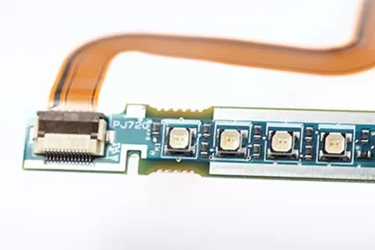
Scrap one misregistered buried via on a 16-layer panel and the entire board is lost — there is no rework path once a sublamination has been pressed. That risk is why selecting among blind and buried vias PCB manufacturers in 2026 matters far more than picking a standard multilayer shop. Sequential lamination, laser-drilled microvias, and via-in-pad plating demand a level of process control most fabricators do not run every day.
This guide ranks ten manufacturers with proven blind and buried via capability, compares their stackup limits, certifications, and turnaround expectations, then walks through the criteria engineers use to qualify a supplier. Whether you are sourcing HDI boards for a wearable, a radar module, or an avionics controller, the list covers quick-turn prototype shops and high-volume producers alike. Here is how the field stacks up.
Blind & Buried Vias PCB Manufacturers at a Glance
Company
HQ
Specialty
Best For
Lead Time
PCBSync
Shenzhen
Aerospace-grade HDI, RF/microwave
Defense and aerospace programs
Quick-turn to program-based
TTM Technologies
Santa Ana, CA, USA
1–56 layer HDI fab + turnkey assembly
One-stop prototype-to-volume builds
Quick-turn available
AT&S
Leoben, Austria
Any-layer HDI, IC substrates
Automotive and medical HDI at scale
Program-based
Ibiden
Ogaki, Japan
Package substrates, fine-line HDI
High-end computing and mobile
Program-based
Unimicron
Taoyuan, Taiwan
Any-layer HDI, carrier boards
Consumer and networking volume
Program-based
Würth Elektronik
Niedernhall, Germany
Microvia HDI, European quick-turn
EU prototypes and mid-volume
Quick-turn available
Zhen Ding Technology
Taoyuan, Taiwan
SLP, flex, and HDI at scale
Smartphone-class volume
Program-based
Summit Interconnect
Anaheim, CA, USA
ITAR rigid and rigid-flex HDI
US defense quick-turn
Quick-turn available
NCAB Group
Stockholm, Sweden
Managed HDI sourcing
Audited multi-factory supply
Standard
Sanmina
San Jose, CA, USA
High-reliability HDI + EMS
Regulated, vertically integrated builds
Program-based
Selection Methodology
Rankings weigh five factors: documented blind and buried via capability (sequential lamination depth, laser microvia formation, via-in-pad and filled-via options); quality certifications such as ISO 9001 and conformance to IPC standards like IPC-6012; breadth of industries served, since automotive, medical, and aerospace audits stress-test a fab differently than consumer work; publicly verifiable customer base and scale; and geographic fit for prototyping versus volume. Where a company does not publish a specification, the entry stays general rather than guessing. Positions reflect capability fit for blind and buried via work, not overall company size.
1. PCBSync
PCBSync is a Shenzhen-based one-stop supplier founded in 2005 that combines PCB fabrication, assembly, and components sourcing under one roof — useful when a blind and buried via design also needs SMT, BGA rework capability, and a managed BOM. Fabrication spans 1–56 layers across FR4, HDI, flex, rigid-flex, Rogers, ceramic, aluminum, copper-core, and heavy copper constructions, so complex via structures can be quoted alongside exotic materials in a single DFM pass.
•Founded / HQ: 2005; Shenzhen, China — 20+ years in operation
•Key Services: Turnkey PCB manufacturing, SMT/THT/BGA and mixed-technology assembly, box build, cable harness, components sourcing
•Notable Capabilities: 1–56 layer stackups including HDI and rigid-flex; ISO 9001, IPC-A-610 Class 3, RoHS; testing via AOI, X-ray, ICT, flying probe, 3D SPI, and functional test — X-ray matters for inspecting buried via and BGA joints
•Industries Served: Automotive, medical, aerospace, industrial, IoT, robotics, telecom, drone, military; publicly listed customers include Honeywell, Siemens Healthineers, Analog Devices, Continental, and Fermilab
•Best For: Teams that want fabrication, assembly, and sourcing handled by one accountable supplier from prototype through volume.
2. TTM Technologies
TTM Technologies is the largest PCB fabricator in North America and a default candidate when blind and buried via boards must survive defense qualification. The company pairs sequential lamination HDI with deep RF and microwave expertise, which matters for radar and phased-array work where buried vias sit beneath controlled-impedance structures. With plants in both North America and Asia, TTM can keep ITAR builds domestic while moving cost-sensitive volume offshore.
•Founded / HQ: 1998; Santa Ana, California, USA
•Key Services: Rigid PCB fabrication, rigid-flex, RF/microwave builds, backplanes, engineering support for complex stackups
•Notable Capabilities: Stacked and staggered laser microvias, sequential lamination HDI, AS9100- and ITAR-registered sites, high layer counts for avionics-class boards
•Industries Served: Aerospace & defense, medical, networking, data center computing, automotive
•Best For: Defense and aerospace programs that need export-controlled, domestically fabricated HDI.
3. AT&S
Austria’s AT&S helped commercialize any-layer HDI — the construction where every layer pair connects through stacked microvias — and remains one of the most advanced blind and buried via fabricators in Europe. Founded in 1987 and headquartered in Leoben, it runs production sites across Austria and Asia, including major plants in Chongqing and Kulim, and has pushed into IC substrates where via geometries shrink even further.
•Founded / HQ: 1987; Leoben, Austria
•Key Services: HDI and any-layer HDI fabrication, IC substrates, embedded component packaging
•Notable Capabilities: Stacked microvia constructions, high-volume automotive-qualified HDI lines, substrate-like geometries
•Industries Served: Automotive, medical, industrial, aerospace, mobile devices
•Best For: Automotive and medical OEMs that need European engineering with Asian-scale capacity.
4. Ibiden
Japan’s Ibiden has operated since 1912 and today sits at the top tier of package substrate and fine-line HDI manufacturing. Its substrate work for high-performance processors uses via structures considerably smaller than standard PCB blind vias, and that precision carries over to its high-density board business. Ibiden is a program supplier: it engages on sustained, high-volume products rather than small prototype lots.
•Founded / HQ: 1912; Ogaki, Gifu, Japan
•Key Services: IC package substrates, high-density multilayer boards, fine-line HDI
•Notable Capabilities: Ultra-fine via and line geometries, substrate-class registration accuracy, large-scale automated production
•Industries Served: High-performance computing, data center, mobile, automotive electronics
•Best For: High-end computing and mobile programs with sustained volume.
5. Unimicron
Founded in 1990 in Taoyuan, Unimicron ranks among the world’s largest PCB producers and runs any-layer HDI alongside IC carrier production. Its German operation gives it a rare combination: Taiwanese and Chinese volume plants plus a European site for customers who need regional supply. For blind and buried via work, Unimicron’s strength is repeatability at enormous scale rather than boutique engineering.
•Founded / HQ: 1990; Taoyuan, Taiwan
•Key Services: HDI and any-layer HDI, conventional multilayer, IC carriers, flex
•Notable Capabilities: High-volume stacked microvia production, carrier-grade fine features, multi-region manufacturing footprint
•Industries Served: Networking, consumer electronics, computing, automotive
•Best For: Buyers consolidating high-volume HDI demand with one large-scale supplier.
6. Würth Elektronik
The circuit board arm of Germany’s Würth Group, with roots back to 1971, Würth Elektronik runs three German production sites and has built its reputation on quick-turn prototypes and mid-volume HDI. Its microvia and buried via offering is aimed at engineers who want a fab they can call — design reviews happen in European time zones, and small lots are welcome rather than tolerated.
•Founded / HQ: 1971 (circuit board operations); Niedernhall, Germany
•Key Services: Quick-turn prototyping, HDI microvia fabrication, multilayer and flex production, design support
•Notable Capabilities: Laser-drilled blind vias, buried via multilayers, three German plants for short logistics chains
•Industries Served: Industrial, automotive, medical, energy, research institutions
•Best For: European teams iterating prototypes that need fast, local engineering feedback.
7. Zhen Ding Technology
Founded in 2006 and affiliated with Foxconn, Taiwan’s Zhen Ding has grown into one of the world’s largest PCB makers by revenue. Its core strength is substrate-like PCB (SLP) and flex production for smartphone-class customers — territory where blind and buried microvias are not a premium option but the baseline construction on every panel. Zhen Ding is built for volume measured in millions of units.
•Founded / HQ: 2006; Taoyuan, Taiwan
•Key Services: SLP, flexible PCBs, HDI rigid boards, IC substrates
•Notable Capabilities: mSAP fine-line processing, stacked microvia structures at consumer-electronics scale, massive automated capacity
•Industries Served: Smartphones, wearables, tablets, automotive, servers
•Best For: Consumer electronics programs at smartphone-class volume.
8. Summit Interconnect
Summit Interconnect, founded in 2016 in Anaheim, has assembled multiple US fabrication sites through acquisition and focused them on defense, space, and high-reliability work. The company is ITAR-registered and built around complex rigid and rigid-flex boards — exactly the constructions where blind and buried vias intersect with sequential lamination and tight registration budgets. Its pitch is domestic quick-turn for designs other shops no-bid.
•Founded / HQ: 2016; Anaheim, California, USA
•Key Services: Complex rigid PCB fabrication, rigid-flex, quick-turn prototyping for high-reliability programs
•Notable Capabilities: ITAR-registered US facilities, sequential lamination, blind/buried via rigid-flex constructions
•Industries Served: Defense, space, medical, industrial
•Best For: US programs needing fast domestic turns on complex, export-controlled boards.
9. NCAB Group
Stockholm-based NCAB, founded in 1993 and listed on Nasdaq Stockholm, does not own factories — it manages them. Its engineers audit and qualify Asian fabs, then place customer orders into the factory whose blind and buried via process best fits each design. For buyers without the resources to audit a Shenzhen HDI line themselves, NCAB sells exactly that oversight, with local technical staff across Europe, Asia, and the Americas.
•Founded / HQ: 1993; Stockholm, Sweden
•Key Services: Managed PCB sourcing, factory auditing and qualification, design-for-manufacturing review
•Notable Capabilities: Multi-factory HDI access, on-the-ground factory management teams in Asia, consistent documentation across suppliers
•Industries Served: Industrial, automotive, medical, telecom across many mid-size OEMs
•Best For: Companies wanting audited Asian HDI capacity without managing fabs directly.
10. Sanmina
Sanmina, founded in 1980 in San Jose, is one of the few global EMS providers that still fabricates its own advanced PCBs, with manufacturing spread across roughly 20 countries. That vertical integration lets it design a blind and buried via stackup, fabricate it, assemble it, and test the finished system under one quality umbrella — attractive for regulated products where supplier handoffs create audit risk.
•Founded / HQ: 1980; San Jose, California, USA
•Key Services: PCB fabrication, full EMS assembly, backplanes, system integration and test
•Notable Capabilities: In-house advanced multilayer and HDI fab, vertically integrated build flow, global footprint of plants
•Industries Served: Medical, defense and aerospace, communications, industrial, automotive
•Best For: Regulated programs that want fabrication and system assembly inside one supplier.
How to Choose the Right Blind & Buried Vias PCB Manufacturer for Your Project
Certifications & Compliance
Start with ISO 9001 as the floor, then match certifications to your market: IPC-6012 Class 3 acceptance for high-reliability boards, AS9100 and ITAR for aerospace and defense, ISO 13485 for medical. Ask for the certificate, not the logo.
Capability Match
Blind and buried via designs live or die on three numbers: how many sequential laminations the fab supports, its minimum laser-drilled microvia diameter, and its registration tolerance between sublaminations. A PCB manufacturer should be able to show a capability matrix with these figures and examples of shipped stackups similar to yours — if the answer is vague, the yield risk lands on you.
Lead Time & Turnaround
Every sequential lamination cycle adds drilling, plating, and pressing steps, so an 8-layer board with buried vias takes longer than a standard 8-layer. Confirm quoted lead times account for your specific via structure, not the fab’s generic multilayer schedule.
Pricing Model & MOQ
Some fabs price prototypes nearly at cost to win production; others charge heavy NRE up front. Clarify minimum order quantities, panelization assumptions, and whether via filling and via-in-pad are line items or included.
Communication & Engineering Support
A serious supplier flags stackup problems during DFM, before tooling. Look for fabs that return marked-up stackup drawings and impedance models, and that answer engineering questions in days, not weeks.
Industry Experience
A fab that ships automotive or medical boards every week has survived audits that consumer-only shops never face. Match the supplier’s audit history to your own compliance burden.
Scalability from Prototype to Production
Re-qualifying a new fab mid-program is expensive. Prefer suppliers — or managed-sourcing partners — that can carry the same stackup from 5 prototypes to 50,000 units without changing the process recipe.
Frequently Asked Questions
What is the difference between blind and buried vias?
A blind via connects an outer layer to one or more inner layers without passing through the whole board. A buried via connects inner layers only and is invisible from either surface. Both free up outer-layer routing space and shrink the board, but both require sublamination steps that standard through-hole-only boards skip.
Do blind and buried vias increase PCB cost?
Yes. Each sequential lamination adds a drill, plate, and press cycle, and laser microvia drilling is billed separately from mechanical drilling. Expect a meaningful premium over a same-layer-count through-hole board — the exact uplift depends on the stackup, so get quotes on your real design rather than relying on rules of thumb.
How many sequential laminations can a board support?
Most capable fabs comfortably run two to three sequential lamination cycles; advanced HDI lines go further with any-layer constructions. Each added cycle compounds registration error and cost, so designers usually keep cycles to the minimum the routing density demands.
What certifications should a blind and buried via manufacturer have?
ISO 9001 at minimum, with fabrication acceptance to IPC-6012 and assembly workmanship to IPC-A-610 — Class 3 for high-reliability products. Add AS9100 or ITAR registration for defense work and ISO 13485 for medical devices.
Can I get a quote without a finished design?
Usually, yes. Most fabs will quote from a preliminary stackup, layer count, board outline, and estimated via structure, then refine pricing once Gerbers and drill files arrive. Early engagement also lets the fab steer your stackup toward its sweet spot before the design hardens.
Is it cheaper to manufacture HDI PCBs in China?
Generally, Chinese HDI fabrication carries lower unit prices and strong quick-turn options, while domestic US or European production wins on export-control compliance, IP sensitivity, and logistics. Many teams prototype regionally and move volume to Asia once the design is stable.
Choosing Your PCB Partner
The right pick among blind and buried vias PCB manufacturers depends on what your program actually stresses: TTM and Summit for export-controlled defense work, AT&S, Ibiden, Unimicron, and Zhen Ding for high-volume any-layer HDI, Würth Elektronik for European quick-turns, NCAB for managed sourcing, and Sanmina for vertically integrated regulated builds. For teams that want fabrication, assembly, and component sourcing handled together — with IPC-A-610 Class 3 workmanship and X-ray inspection of buried structures — PCBSync is a strong one-stop option from prototype through volume.
Shortlist two or three suppliers, send the same stackup to each, and compare the DFM feedback as closely as the price. Request a quote from a vetted manufacturer like PCBSync to benchmark turnaround and pricing for your project.